
Light-Controlled One-Sided Growth of Large Plasmonic Gold Domains on Quantum Rods Observed on the Single Particle Level
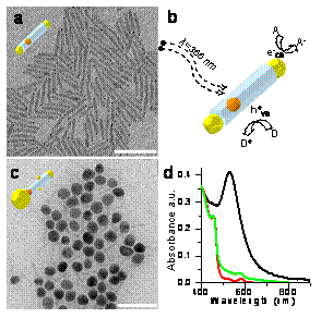
We create large gold domains (up to 15 nm) exclusively on one side of CdS or CdSe/CdS quantum rods by photoreduction of gold ions under anaerobic conditions. Electrons generated in the semiconductor by UV stimulation migrate to one tip where they reduce gold ions. Large golddomains eventually form; these support efficient plasmon oscillations with a light scattering cross section large enough to visualize single hybrid particles in a dark-field microscope during growth in real time.
'Light-Controlled One-Sided Growth of Large Plasmonic Gold Domains on Quantum Rods Observed on the Single Particle Level'
L. Carbone, A. Jakab, Y. Khalavka, C. Sönnichsen
Growth of Gold Tips onto Hyperbranched CdTe Nanostructures
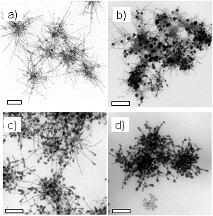
Here, we report the synthesis of a novel metal–semiconductor hybrid based on hyperbranched CdTe particles. These particlesare considerably larger and more complex than the previously reported CdSe and CdS hybrid particles. Goldparticles have been grown selectively onto the tips of preformedsemiconductor substrates at room temperature in air.The gold-tipped hyperbranched particles not only provide intriguinginsight into the level of control of inorganic hybridnanomaterials, but may also enable the creation of blendswith organic molecules for the eventual fabrication of novel electronic and optical materials. We propose a chemical reactionpathway supported by detailed spatially resolved elementalanalysis and control experiments.
'Growth of Gold Tips onto Hyperbranched CdTe Nanostructures'
Y. Khalavka, C. Sönnichsen